


This plan includes
- Instant access to 11,000+ online courses
- Play & Pause Course Videos
 HD Video Recorded Lectures
- Learn on Mobile/PC/Tablet
- Quizzes and Real Projects
- Lifetime Course Certificate
- Instructor Chat Support
- Cancel Plan Anytime
This plan includes
- Instant access to 11,000+ online courses
- Play & Pause Course Videos
- HD Video Recorded Lectures
- Learn on Mobile/PC/Tablet
- Quizzes and Real Projects
- Lifetime Course Certificate
- Instructor Chat Support
- Cancel Plan Anytime
What you'll learn?
- You will learn Basic Electronics Theory, Circuit Design and Analysis, Basics of Printed Circuit Board, Electronic Components and Instruments. Study notes given.
- You will work on Printed Circuit Board Layout Design such as Schematic creation, Library Creation: Electronic Symbol and Package (Footprint Creation) Designing.
- Switching schematic to Board Design (Netlist Creation), Thorough knowledge on Constraint Management Settings, Board Shape Creation (DXF import included) & DRC.
- Work on Single sided Board Design, Double sided Board Design, Via creation and application. Routing on Top and Bottom Layer includes enough practice modules.
- Plan Creation of Power and Ground. Also Split Plan Creation. Design Rule Checking and DRC updates. Work on Artwork. Setting up all required film layer setups.
Course Overview
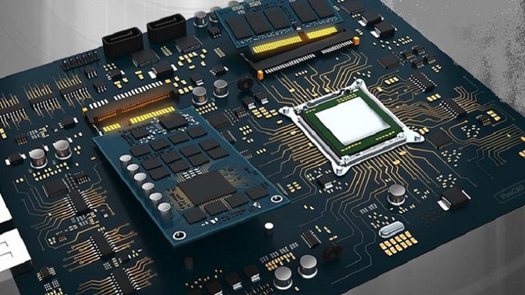
PCB Design and electronics circuit are basements for all type of electronics products. PCBs are derived from the analog and digital circuits which are prepared according to the application required. Printed circuit boards are the main pillars of the Electronics world. Every Electronics products has PCB inside it, from consumer gadgets like computers, smart phones and gaming consoles to industry and even high-tech products.
Required eligibility:
· Diploma in Electrical or Electronics & Communication.
· BE/BTech. in Electrical or Electronics & Communication.
· BSc/MSc in Electronics & Communication.
· ME/MTech. (E&CE) in Communication.
PCB Design Course Content is given below in brief:
Schematic Design:
· Basic Electronics theory.
· Basics of Circuit designing.
· Schematic design preparation.
· Schematic part editing and creation.
· Net list and Net class creation.
· Bill Of Material generation (BOM).
· Electrical Rule Checking.
Footprint Creation:
· Through hole footprint creation.
· Surface Mount Device footprint creation.
· BGA/PGA footprint creation.
Board Designing:
· Board size and shape creation.
· Component placements.
· PCB Routing: Multi-Layer routing.
· Plane creation.
· Design rule checking.
· Gerber generation.
Skills you gain after the course completion:
· Basic Electronics and Electronic components expertise.
· Circuit Designing (Power management circuit designing)
· Circuit Simulation for best understanding of the subject.
· Tools/Software Expertise.
· Basic design module practice up to 2-Layers.
· Advanced design module practice up to 6-Layers.
· Design expertise:
o Assignments consists single and double sided PCB.
o Assignments consists 2-Layers to 6-Layers design.
· Library Module:
o Symbol and Footprint design for all types of packages.
· Placements & Routing techniques.
· Gerber Creating.
Benefits of choosing PCB Design Course:
· Strong hold in basic electronics.
· Circuit Design capability.
· Circuit analysis & ERC.
· Components knowledge.
· Power Supply designing.
· PCB-CAD tool expertise.
· Expert in library creation.
· Multi-layer PCB designing.
· Gerber Creation.
Pre-requisites
- Basic Electronics knowledge, BSc(Electronics), Diploma (Electronics or Electrical), BE (Electronics or Electrical), Master degree in Electronics and Electrical.
- If you are working in PCB Manufacturing and Assembly unit, PCB Design course will be an added skillset to your career profile.
- If you own PCB printing, assembly and component soldering unit, you can learn PCB Design and can extend your business unit towards service sector.
- If you have passion on Electronics subject, you can enroll this course and convert your passion into career.
Target Audience
- Diploma in Electronics and Communication, Diploma in Electronics and Electrical and Diploma in Electrical.
- Bachelor of Engineering in Electronics and Communication, Bachelor of Engineering in Electrical and Electronics.
- BSc in Electronics, MSc in Electronics, MS in Electronics and Post graduate in Electronics and communication.
- Hardware designers, PCB manufacturer, Electronic Components engineer, PCB design and developers.
- Circuit designers, Embedded engineers and Beginners interested in development of PCB
Curriculum 167 Lectures 19:59:35
-
Section 1 : Introducing OrCAD/Allegro of Cadence software
- Lecture 2 :
- Things We Learn Here...
- Lecture 3 :
- OrCAD Environment and Initialize new project Part 1
- Lecture 4 :
- OrCAD Environment and Initialize new project Part 2
- Lecture 5 :
- OrCAD Capture - Schematic Page Property
- Lecture 6 :
- Working with Colors and Grid Display Part 1
- Lecture 7 :
- Pan and Zoom Settings in OrCAD
- Lecture 8 :
- Working with Colors and Grid Display Part 2
- Lecture 9 :
- Selection Area Pre-Settings
- Lecture 10 :
- Line and Shape Properties in OrCAD
- Lecture 11 :
- Working with Colors and Grid Display Part 3
- Lecture 12 :
- Design Templates in OrCAD
- Lecture 13 :
- Auto Back Ups in Capture
- Lecture 14 :
- Working with Windows Cascade Tiling and Session logs
- Lecture 15 :
- Accessories of Cadence Utilities
-
Section 2 : Electronic Symbol Library Creation : IEEE Standard
- Lecture 1 :
- Introduction to Electronic Symbol Library
- Lecture 2 :
- How to Make IEEE Standard Electronic Symbols Part 1
- Lecture 3 :
- How to Make IEEE Standard Electronic Symbols Part 2
- Lecture 4 :
- How to Make IEEE Standard Electronic Symbols Part 3
- Lecture 5 :
- How to Make IEEE Standard Electronic Symbols Part 4
- Lecture 6 :
- How to Make IEEE Standard Electronic Symbols Part 5
- Lecture 7 :
- How to Make IEEE Standard Electronic Symbols Part 6
- Lecture 8 :
- How to Make IEEE Standard Electronic Symbols Part 7
- Lecture 9 :
- How to Make IEEE Standard Electronic Symbols Part 8
- Lecture 10 :
- How to Make IEEE Standard Electronic Symbols Part 9
- Lecture 11 :
- How to Make IEEE Standard Electronic Symbols Part 10
- Lecture 12 :
- How to Make IEEE Standard Electronic Symbols Part 11
- Lecture 13 :
- How to Make IEEE Standard Electronic Symbols Part 12
- Lecture 14 :
- How to Make IEEE Standard Electronic Symbols Part 13
- Lecture 15 :
- How to Make IEEE Standard Electronic Symbols Part 14
- Lecture 16 :
- Symbol Creation of ICs using Spread Sheet and Regular Methods Part 1
- Lecture 17 :
- Symbol Creation of ICs using Spread Sheet and Regular Methods Part 2
- Lecture 18 :
- Symbol Creation of ICs using Spread Sheet and Regular Methods Part 3
- Lecture 19 :
- Symbol Creation of ICs using Spread Sheet and Regular Methods Part 4
- Lecture 20 :
- Symbol Creation of ICs using Spread Sheet and Regular Methods Part 5
- Lecture 21 :
- What are Heterogeneous Symbol Creation and How to Make it Part 1
- Lecture 22 :
- What are Heterogeneous Symbol Creation and How to Make it Part 2
- Lecture 23 :
- What are Heterogeneous Symbol Creation and How to Make it Part 3
- Lecture 24 :
- What are Heterogeneous Symbol Creation and How to Make it Part 4
- Lecture 25 :
- What are Heterogeneous Symbol Creation and How to Make it Part 5
-
Section 3 : An Introduction to Schematic Creation: OrCAD Capture
- Lecture 1 :
- Lets Begin New Project Schematic Preparation Part 1
- Lecture 2 :
- Lets Begin New Project Schematic Preparation Part 2
- Lecture 3 :
- Lets Begin New Project Schematic Preparation Part 3
- Lecture 4 :
- Lets Begin New Project Schematic Preparation Part 4
- Lecture 5 :
- Lets Begin New Project Schematic Preparation Part 5
- Lecture 6 :
- Wiring Net Naming and Global Connections Part 1
- Lecture 7 :
- Wiring Net Naming and Global Connections Part2
- Lecture 8 :
- Multi-Page Schematic Preparation Part 1
- Lecture 9 :
- Multi-Page Schematic Preparation Part 2
- Lecture 10 :
- Learn Busses and Off-Page Connectors Part 1
- Lecture 11 :
- Learn Busses and Off-Page Connectors Part 2
- Lecture 12 :
- Electrical Rule Checking (ERC) Part 1
- Lecture 13 :
- Electrical Rule Checking (ERC) Part 2
- Lecture 14 :
- Electrical Rule Checking (ERC) Part 3
- Lecture 15 :
- Electrical Rule Checking (ERC) Part 4
- Lecture 16 :
- Bill of Material (BOM) Preparation Part 1
- Lecture 17 :
- Bill of Material (BOM) Preparation Part 2
- Lecture 18 :
- Bill of Material (BOM) Preparation Part 3
- Lecture 19 :
- Bill of Material (BOM) Preparation Part 4
- Lecture 20 :
- Bill of Material (BOM) Preparation Part 5
- Lecture 21 :
- Bill of Material (BOM) Preparation Part 6
- Lecture 22 :
- Bill of Material (BOM) Preparation Part 7
- Lecture 23 :
- Bill of Material (BOM) Preparation Part 8
-
Section 4 : Footprint Creation of Electronics Components
- Lecture 1 :
- An Introduction to Electronic Components Footprints
- Lecture 2 :
- What is Padstack Editor and Know Padstack Environment Part 1
- Lecture 3 :
- What is Padstack Editor and Know Padstack Environment Part 2
- Lecture 4 :
- Decoding Imperial and Metric Codes and Unit Conversions Part 1
- Lecture 5 :
- Decoding Imperial and Metric Codes and Unit Conversions Part 2
- Lecture 6 :
- An understanding of Solderpad Solderpaste and Soldermask Part 1
- Lecture 7 :
- An understanding of Solderpad Solderpaste and Soldermask Part 2
- Lecture 8 :
- Creating a Solder pad of Surface Mount Device using Padstack Editor Part 1
- Lecture 9 :
- Creating a Solder pad of Surface Mount Device using Padstack Editor Part 2
- Lecture 10 :
- Creating a Solder pad of Surface Mount Device using Padstack Editor Part 3
- Lecture 11 :
- Introduction to PCB Editor for Footprint creation and Default Setups Part 1
- Lecture 12 :
- Introduction to PCB Editor for Footprint creation and Default Setups Part 2
- Lecture 13 :
- Introduction to PCB Editor for Footprint creation and Default Setups Part 3
- Lecture 14 :
- Pad Positioning in Footprint Creation using PCB Editor Part 1
- Lecture 15 :
- Pad Positioning in Footprint Creation using PCB Editor Part 2
- Lecture 16 :
- Pad Positioning in Footprint Creation using PCB Editor Part 3
- Lecture 17 :
- Assembly Drawing Methods and Tips Part 1
- Lecture 18 :
- Assembly Drawing Methods and Tips Part 2
- Lecture 19 :
- Assembly Drawing Methods and Tips Part 3
- Lecture 20 :
- Silkscreen Drawing Methods and Tips Part 1
- Lecture 21 :
- Silkscreen Drawing Methods and Tips Part 2
- Lecture 22 :
- Silkscreen Drawing Methods and Tips Part 3
- Lecture 23 :
- Place Bound Drawing Methods and Assign Component Hight
- Lecture 24 :
- Know about Design For Assembly (DFA) and its rules
- Lecture 25 :
- Route Restriction on Footprint level
- Lecture 26 :
- SMD Footprint design complete process Part 1
- Lecture 27 :
- SMD Footprint design complete process Part 2
- Lecture 28 :
- PTH Footprint design complete process Part 1
- Lecture 29 :
- PTH Footprint design complete process Part 2
- Lecture 30 :
- PTH Footprint design complete process Part 3
- Lecture 31 :
- SMD Footprint using Package Symbol Wizard Part 1
- Lecture 32 :
- SMD Footprint using Package Symbol Wizard Part 2
- Lecture 33 :
- PTH Footprint using Package Symbol Wizard Part 1
- Lecture 34 :
- PTH Footprint using Package Symbol Wizard Part 2
- Lecture 35 :
- Male Header Footprint Creation for Single Row Part 1
- Lecture 36 :
- Male Header Footprint Creation for Single Row Part 2
- Lecture 37 :
- Male Header Footprint Creation for Single Row Part 3
- Lecture 38 :
- Male Header Footprint Creation for Double Row Part 1
- Lecture 39 :
- Male Header Footprint Creation for Double Row Part 2
- Lecture 40 :
- Single In Line Package Footprint Creation using Wizard Part 1
- Lecture 41 :
- Single In Line Package Footprint Creation using Wizard Part 2
- Lecture 42 :
- SOT-223 Footprint Creation Part 1
- Lecture 43 :
- SOT-223 Footprint Creation Part 2
- Lecture 44 :
- SOT-223 Footprint Creation Part 3
- Lecture 45 :
- SOIC Footprint Creation using Package Wizard Part 1
- Lecture 46 :
- SOIC Footprint Creation using Package Wizard Part 2
- Lecture 47 :
- SOIC Footprint Creation using Package Wizard Part 3
- Lecture 48 :
- PDIP Footprint Creation using Package Wizard Part 1
- Lecture 49 :
- PDIP Footprint Creation using Package Wizard Part 2
- Lecture 50 :
- PDIP Footprint Creation using Package Wizard Part 3
- Lecture 51 :
- Editing Pads on Footprint Level
- Lecture 52 :
- PLCC Footprint Creation using Wizard Part 1
- Lecture 53 :
- PLCC Footprint Creation using Wizard Part 2
- Lecture 54 :
- PLCC Footprint Creation using Wizard Part 3
- Lecture 55 :
- Ball Grid Array Full Matrix Footprint Creation Part 1
- Lecture 56 :
- Ball Grid Array Full Matrix Footprint Creation Part 2
- Lecture 57 :
- Ball Grid Array Perimeter Matrix Footprint Creation
- Lecture 58 :
- Assignments
-
Section 5 : Switching to Printed Circuit Board Design (PCB Design)
- Lecture 1 :
- Assigning Footprints to Schematic Circuit Part 1
- Lecture 2 :
- Assigning Footprints to Schematic Circuit Part 2
- Lecture 3 :
- Assigning Footprints to Schematic Circuit Part 3
- Lecture 4 :
- Assigning Footprints to Schematic Circuit Part 4
- Lecture 5 :
- Assigning Footprints to Schematic Circuit Part 5
- Lecture 6 :
- Assigning Footprints to Schematic Circuit Part 6
- Lecture 7 :
- Assigning Footprints to Schematic Circuit Part 7
- Lecture 8 :
- Assigning Footprints to Schematic Circuit Part 8
- Lecture 9 :
- Assigning Footprints to Schematic Circuit Part 9
- Lecture 10 :
- Assigning Footprints to Schematic Circuit Part 10
- Lecture 11 :
- Pins and Pads Mapping before switching Part 1
- Lecture 12 :
- Detailed explanation of Pins and Pads Mapping Part 1
- Lecture 13 :
- Detailed explanation of Pins and Pads Mapping Part 2
- Lecture 14 :
- Detailed explanation of Pins and Pads Mapping Part 3
- Lecture 15 :
- Switching from Schematics to Board Design
- Lecture 16 :
- Pins and Pads Mapping before switching Part 2
-
Section 6 : Board Shapes and Board Restrictions
- Lecture 1 :
- Working with PCB Board Shape Part 1
- Lecture 2 :
- Working with PCB Board Shape Part 2
- Lecture 3 :
- Working with PCB Board Shape Part 3
- Lecture 4 :
- Working with PCB Board Shape Part 4
- Lecture 5 :
- Working with PCB Board Shape Part 5
- Lecture 6 :
- DXF Import and Export in Board Shapes Part 1
- Lecture 7 :
- DXF Import and Export in Board Shapes Part 2
- Lecture 8 :
- Know about Package Keepin in Board Design
- Lecture 9 :
- Know about Route Keepin in Board Design
- Lecture 10 :
- Convert from Board outline to Design Outline Part 1
- Lecture 11 :
- Component Import on Board Part 1
- Lecture 12 :
- Convert from Board outline to Design Outline Part 2
- Lecture 13 :
- Component Import on Board Part 2
-
Section 7 : Placements on PCB
- Lecture 1 :
- Non Plated Thru Hole (NPTH) Creation
- Lecture 2 :
- How to import Non Plated Thru hole (NPTH) ? Part 1
- Lecture 3 :
- How to import Non Plated Thru hole (NPTH) ? Part 2
- Lecture 4 :
- How to Place Components Manually Part 1
- Lecture 5 :
- How to Place Components Manually Part 2
- Lecture 6 :
- How to Place Components Manually Part 3
- Lecture 7 :
- What are Rooms and How to Create Rooms
- Lecture 8 :
- Create Room property in Schematic and Placement in Allegro - Part 1
- Lecture 9 :
- Create Room property in Schematic and Placement in Allegro - Part 2
- Lecture 10 :
- Create Room property in Schematic and Placement in Allegro - Part 3
- Lecture 11 :
- Create Room property in Schematic and Placement in Allegro - Part 4
- Lecture 12 :
- Create Room property in Schematic and Placement in Allegro - Part 5
- Lecture 13 :
- Create Room property in Schematic and Placement in Allegro - Part 6
- Lecture 14 :
- Create Room property in Schematic and Placement in Allegro - Part 7
- Lecture 15 :
- Place Replicate Creation and Apply Part 1
- Lecture 16 :
- Place Replicate Creation and Apply Part 2
- Lecture 17 :
- Place Replicate Creation and Apply Part 3
Our learners work at
Frequently Asked Questions
-
How do i access the course after purchase?
It's simple. When you sign up, you'll immediately have unlimited viewing of thousands of expert courses, paths to guide your learning, tools to measure your skills and hands-on resources like exercise files. There’s no limit on what you can learn and you can cancel at any time. -
Are these video based online self-learning courses?
Yes. All of the courses comes with online video based lectures created by certified instructors. Instructors have crafted these courses with a blend of high quality interactive videos, lectures, quizzes & real world projects to give you an indepth knowledge about the topic. -
Can i play & pause the course as per my convenience?
Yes absolutely & thats one of the advantage of self-paced courses. You can anytime pause or resume the course & come back & forth from one lecture to another lecture, play the videos mulitple times & so on. -
How do i contact the instructor for any doubts or questions?
Most of these courses have general questions & answers already covered within the course lectures. However, if you need any further help from the instructor, you can use the inbuilt Chat with Instructor option to send a message to an instructor & they will reply you within 24 hours. You can ask as many questions as you want. -
Do i need a pc to access the course or can i do it on mobile & tablet as well?
Brilliant question? Isn't it? You can access the courses on any device like PC, Mobile, Tablet & even on a smart tv. For mobile & a tablet you can download the Learnfly android or an iOS app. If mobile app is not available in your country, you can access the course directly by visting our website, its fully mobile friendly. -
Do i get any certificate for the courses?
Yes. Once you complete any course on our platform along with provided assessments by the instructor, you will be eligble to get certificate of course completion.
-
For how long can i access my course on the platform?
You require an active subscription to access courses on our platform. If your subscription is active, you can access any course on our platform with no restrictions. -
Is there any free trial?
Currently, we do not offer any free trial. -
Can i cancel anytime?
Yes, you can cancel your subscription at any time. Your subscription will auto-renew until you cancel, but why would you want to?

Instructor

1200 Course Views
4 Courses


